APEX Chipset is the first cloud-native, AI-powered EDA platform purpose-built for sovereign semiconductor design. Full RTL-to-GDSII pipeline — no licence servers, no vendor lock-in, no data leaving your infrastructure.
Over 55 professional EDA tools powered by 6 AI models — accessible through a single REST API. No dongles, no floating licences, no third-party servers. Deploy on sovereign soil with full data control.
6 specialist AI models drive every design stage — GNN4LS graph-based logic synthesis, HeteroGNN neural placement with 12% wirelength reduction, RL-based routing optimisation, and the 229B-parameter Crown Jewel EDA expert for complex optimisation tasks.
Complete front-to-back semiconductor design pipeline. RTL synthesis, AI-driven floorplanning, place and route, clock tree synthesis, DRC/LVS, parasitic extraction, ATPG with 97.3% fault coverage — all from a browser IDE.
ML-KEM-768 post-quantum cryptography, AES-256-GCM at rest, TLS 1.3 in transit, air-gapped on-premise deployment. No data ever leaves sovereign soil. Built to government and defence security standards.
Browser-based IDE with real-time collaboration, versioned project snapshots, team workspaces, and role-based access control. Design from anywhere — deploy on your own infrastructure or sovereign cloud.
Target SkyWater 130nm, TSMC 12nm FinFET, GF 22FDX, or any FPGA family. Custom PDK mapping via JSON configuration. ASIC and FPGA flows from a single codebase with automatic technology mapping.
UAE-incorporated entity (ADGM ADGM), physical semiconductor lab in Abu Dhabi, on-premise Crown Jewel AI inference node, dedicated data centre with geo-redundant failover, and an Emiratised engineering team.
Visual overview of the APEX Chipset ecosystem — from the browser-based EDA IDE to the sovereign data centre infrastructure deployed in the UAE.
Complete sovereign semiconductor platform: 117 API endpoints, 55 EDA tools, 804K gate X1 tapeout, 6 AI models, post-quantum security, and UAE-deployed infrastructure with local engineering team.
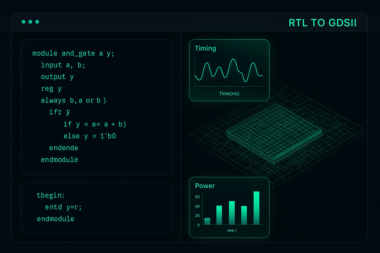
Browser-based full-stack EDA IDE featuring Verilog/VHDL code editor with green-on-black syntax highlighting, integrated 3D chip layout viewer with wireframe overlays, real-time timing analysis graphs, and power consumption monitoring panels.
UAE-hosted sovereign data centre with air-gapped deployment, post-quantum ML-KEM-768 encryption, geo-redundant active-standby failover across two UAE facilities, and dedicated Crown Jewel 229B AI inference on sovereign soil.
Multi-agent AI architecture: GNN4LS for logic synthesis, HeteroGNN neural placement, RL reinforcement learning router, AI PPA Pareto optimiser, ATPG pattern generator, and the Crown Jewel 229B-parameter EDA expert for complex optimisation.
The complete APEX-EDA semiconductor design pipeline — from RTL description to tapeout-ready GDSII — powered by AI at every stage.
Enterprise-grade EDA. Full sovereign deployment. Book a demonstration or start designing today with your free account.